
Designing Circuits for High Density Interconnect
When it comes to designing circuits for high density interconnect, PCB engineers must consider signal transmission, power and grounding, and component placement. Moreover, PCB designers must work within strict design rules and manufacturing constraints in order to achieve optimal performance.
high density interconnect PCBs (HDI) represent a huge leap forward from traditional single- and double-sided PCBs, as they enable larger components to be placed on the board alongside smaller vias and capture pads. Consequently, HDI circuit boards offer increased signal transmission, lower impedance, and minimized crosstalk between adjacent traces. These attributes help ensure that electronic signals are delivered without interference or degradation, resulting in more reliable devices and higher operating frequencies.
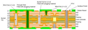
The primary challenge that designers face when working with HDI technology is overcoming the limitations of traditional routing methods. While conventional PCBs can be designed using computer-aided design software, HDI requires advanced routing techniques to make the most of the space available. Fortunately, many of these challenges can be mitigated by utilizing multi-layer boards and advanced fabrication techniques such as laser drilling and plating-through-hole.
Challenges of Designing Circuits for High Density Interconnect
Another challenge that designers face is the difficulty of managing impedance control at high speeds. With higher component pitch and shorter lengths, high-speed signals can be prone to electromagnetic interference (EMI). In order to maintain optimal functioning, high-speed signals must be routed with minimal impedance and optimum signal-to-ground connections. The use of HDI technologies can significantly reduce the number of EMI issues and increase operating speed.
As the demand for high-performance electronics continues to grow, the need for innovative PCBs that can meet these needs becomes increasingly critical. The adoption of HDI and Ultra HDI technologies represents a significant step forward in meeting these requirements. In the video below, Vardya delves into the technical complexities associated with these advances and offers practical insights on how to address them.
The proper layer stacking of a HDI PCB is key to maintaining optimal thermal reliability. It is necessary to create an even distribution of copper across the entire surface area of the board, preventing hotspots that could compromise operational functionality. In addition, the use of thermal vias to conduct heat away from hotspots is essential for improving heat dissipation and reducing temperature fluctuations. Finally, the incorporation of cooling fans can also significantly improve thermal efficiency by facilitating greater airflow and active cooling.