
Manage Trace Routing in Flex Circuit PCBs
While the layer stacks in flex circuits are similar to those of rigid PCBs, it’s not always easy to manage trace routing. Because flex boards are designed to bend, traces need to be routed with care to avoid stress points where they may break, crack or delaminate. The good news is that there are some easy tricks you can use to make a flex circuit layout more resistant to stresses that will cause damage.
First, it is important to use proper trace widths. Trace widths should be consistent across the board so that signals don’t become distorted when they are bended or compressed. Also, be sure to keep sensitive analog signals away from noisy digital ones to avoid interference and signal reflections.
Another trick is to stagger traces on adjacent layers so that they do not overlap. Overlapping traces creates a concentrated area of stress on one side of the flex circuit pcb and increases the chance of shorting during manufacturing. Staggering reduces the tension on the traces and distributes the stress more evenly across the substrate.
Using rounded corners on all of the copper pads on your flex design will also make it more resilient to stress. Sharp corners and other sharp junctures can cause stress cracking during the bending and rolling process used to manufacture flex circuits. To prevent this, use rounded corner shapes instead of square or triangle shaped pads and add plated vias with annular rings that are at least 8 mils in diameter to strengthen connections.
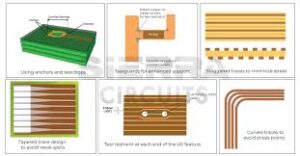
How to Manage Trace Routing in Flex Circuit PCBs
One last tip is to avoid routing traces near areas where the flex circuit is expected to bend. This will protect the traces from being damaged and increase the mechanical performance of your flex circuit design. If this isn’t possible, try using a hatched polygon shape rather than solid copper for the trace and avoiding overlapping traces.
Another important factor to consider is the thickness of your flex circuit material. Flex circuits are typically manufactured with flexible dielectric materials like polyimide or FR4. Choosing the right flex material thickness is critical to minimize stress on the traces and ensure that your flex circuit will perform as intended in the final product. When selecting the flex material, be sure to consult with your manufacturer’s rules and guidelines for thickness selection.
Flex circuits, or flexible printed circuits, offer unparalleled versatility and space-saving benefits compared to traditional rigid PCBs (printed circuit boards). They are particularly useful in applications requiring complex geometries or movement, such as in wearable electronics or compact consumer devices. However, the unique characteristics of flex circuits pose distinct challenges for trace routing. Effective trace routing is crucial for ensuring signal integrity, durability, and overall performance of the circuit. Here’s a comprehensive guide on how to manage trace routing in flex circuit PCBs.
Flex circuits are made from flexible substrates like polyimide or polyester, which are designed to bend and fold without cracking. The key to managing trace routing is understanding that these substrates have different electrical and mechanical properties compared to rigid PCBs. Flex circuits often include copper traces, which must be routed in a manner that accommodates bending and flexing.