
Flex Circuit PCBs for Aerospace
When used correctly, flex circuit PCBs can be extremely reliable and durable. Compared to rigid circuit boards, they are capable of surviving significant dynamic loads and vibrations, reducing failure rates and increasing overall device longevity. They are also thinner, allowing for increased heat dissipation and airflow. Additionally, they can adapt to small or irregularly shaped spaces that cannot be easily accommodated by rigid circuit boards. This versatility makes them suitable for aerospace applications such as aircraft and spacecraft.
A typical flex circuit pcb is constructed of a flexible substrate with multiple layers of conductive copper and an adhesive-based coverlay that exposes the pads on the copper layer. Using this method of construction, it is possible to reduce the thickness of the PCB by up to 75% while still providing a reliable circuit. These incredibly thin layers are often used in applications where high reliability is needed and where space is limited.
Depending on the design, it may be necessary to add a protective layer to the surface of the flex PCB to prevent damage or moisture penetration. This protective layer can be made of a polyimide film, polyester or other material. In addition, it may be important to include a layer of insulation on the backside of the flex circuit. This will protect the conductors from the stresses of bending and will minimize the potential for corrosion.
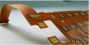
Flex Circuit PCBs for Aerospace Applications
The most common flex circuit substrate is a polyimide (PI) film. This is a thermosetting material that does not soften or change shape when heated, unlike many other thermosetting resins. This makes PI the ideal material for a flex circuit substrate. Other benefits of PI include its high dielectric withstanding voltage, ability to be etched in narrow widths and spacings, resistance to humidity and tears, and the capability of being shielded against EMI and RF absorption or transmission.
Once the flex circuit layout is designed, the fabrication process can begin. Gerber files are sent to the manufacturer and components are placed on the board according to the specifications. The flex PCB can then be tested to make sure it meets the project requirements.
A flex circuit design must be carefully implemented in order to avoid stress points, which can cause failures in the traces and connectors. To help prevent this, the traces should be routed parallel to the flex circuit’s overall bend radius. This will prevent I-beaming of the traces, which is a major cause of copper breakage and failures. The traces should also be staggered, tapering from wide to narrow in a gradual fashion along the flex circuit’s inner curve. This will help to ensure that the flex circuit is able to withstand a large number of bending cycles without failing.
Another important consideration is the choice of conductive material for the copper traces. Standard bare copper foil is notorious for work-hardening and fatigue, so it is not recommended for flex circuits that will be subjected to repeated creasing or movement. When choosing a conductive material for a flex PCB, it is highly recommended that you select rolled-annealed copper. This will increase the cost but will allow the traces to stretch significantly before fatigue cracking occurs. This is particularly important for flex circuits that are subjected to frequent bending.