
blind vias affected by PCB material
Blind vias allow signals to be transferred between layers of the PCB without having to cross the surface of the board. They are usually used in multilayer PCBs and are popular with high-density interconnect PCBs (HDI). This type of circuit board can have more layers and devices on a smaller footprint, resulting in better power delivery and fewer signal interference issues. The use of blind and buried vias also helps to reduce the overall thickness of the circuit board, which can make it thinner and lighter.
PCBs can be made with either blind vias, and they can be produced after or before the lamination process. Typically, the vias are drilled into the core, and then the rest of the board is layered on top. This method allows the designers to create a more complex circuit board with more connections in a smaller space, which is necessary for many electronics products today.
The PCB material properties that are used in the manufacturing of a circuit board will have an effect on how well the blind or buried vias function. For instance, if the circuit board has a high coefficient of thermal expansion, the blind or buried vias will shift more easily, which can result in voids and poor connections. This can cause the circuit board to malfunction and affect its performance. Using a higher-quality PCB design with the same coefficient of thermal expansion can help prevent these problems.
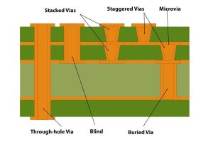
How are blind vias affected by PCB material properties?
Another important factor to consider when designing a PCB with blind or buried vias is the plating process. The copper plating process must be carefully controlled to avoid etching away the underlying layer or creating voids in the hole. This can cause problems in the future, especially if the blind or buried vias are not filled with the proper amount of solder.
Blind or buried vias can be created in a few different ways. Most commonly, they are drilled into the PCB with a CNC machine. The drill bit progressively removes the material to create the desired size of hole and depth. This technique can only achieve a certain level of accuracy, which is why it is used only for the most critical PCBs.
Another way to create blind or buried vias is by laser drilling. This is more expensive than traditional mechanical drilling, but it can produce a more accurate result. This method also requires more time to perform and is usually reserved for specialized applications that require high accuracy. The holes that are created in the PCB are subsequently filled with a conductive ink, which provides good conductivity to the hole walls. The holes can then be plated with copper using electroplating, which fully builds up the metal interconnect between the layers. Regardless of the method of production, blind or buried vias are essential tools for achieving reliable and functional circuit boards. This makes them the ideal choice for electronic devices that need to operate in harsh environments with minimal damage and interference.