
HDI Boards Used in Medical Devices
For medical devices, high performance is crucial. A device that does not function properly may result in a missed diagnosis or even life-threatening consequences. That’s why these devices require extremely reliable components and manufacturing processes. One of the most important components in these devices is the PCB board. To reduce the size of these boards, HDI technology is often used. This technology is used in mobile / cellular phones, touch-screen devices, laptop computers, 4/5G network communications, and military applications such as avionics and smart munitions.
In addition to the need for reliability, medical devices must also be small and lightweight in order to accommodate users and remain comfortable for use. This requires high-density circuitry that enables more functionality to be packed into a smaller space without sacrificing performance standards. The ability of HDI PCBs to deliver advanced features in a compact design makes them ideal for medical and wearable technologies.
Among the most common applications of HDI PCBs are in healthcare, especially in implantable devices like pacemakers and cochlear implants. These devices must meet strict size, power, and performance requirements while remaining safe for long-term use inside the body. A custom-designed hdi board is able to fit these requirements, enabling manufacturers to produce devices that offer life-saving capabilities in a small form factor.
HDI boards are able to achieve these impressive size and performance standards by optimizing the interconnections between layers and components. This is accomplished by utilizing techniques such as laser-drilled microvias, which allow connections between the inner layers to be made through holes smaller than those found on standard PCBs. The use of blind and buried vias also helps to decrease the overall thickness of the board, further reducing its size.
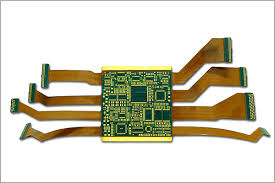
How Are HDI Boards Used in Medical Devices?
To make these complex connections, manufacturers utilize a sequential lamination process that starts with the etching of the inner copper layers. Then, the etched layers are separated by partially cured laminates and stacked together with layers of prepreg on top and bottom. The stack-up is then pressed and heated, which liquifies the prepreg and allows it to stick to the underlying layers of the board. The process of lamination is repeated for each layer of the board, with a total of 6 or more layers in an HDI design.
In addition to the layered structure of HDI PCBs, they also utilize special materials that help to improve their electrical performance. These materials typically include FR-4, which is most commonly used in medical PCBs due to its cost-efficiency and straightforward manufacturing process. However, some medical devices require the use of higher-risk laminates such as polyimide, Teflon, or ceramics, which have a lower dielectric constant and therefore reduce signal loss.
As the demand for more and better technology continues to grow, it is vital that medical devices can provide patients with the advanced functionality they need. HDI PCBs are playing a key role in the growth of both medical and wearable technologies, and their continued advancements will continue to enable new innovations in both fields. To learn more about how a custom-designed HDI board can benefit your application, speak with a PCB manufacturer who offers this cutting-edge technology.